
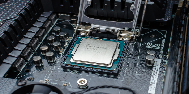
With the development of world’s first chip using 2 nm nanosheet technology, IBM announced a breakthrough in semiconductor design and operation. The new design is expected to outperform today’s 7 nm chips by 45 percent while using 75 percent less energy.
This latest frontier in chip technology, according to IBM, would help accelerate AI, 5G and 6G, edge computing, autonomous vehicles, space exploration, and quantum computing, as well as expand the roadmap for IBM’s own technology offerings, such as IBM Power Systems and IBM Z platforms.
In 2015, IBM revealed the world’s first 7-nanometer test chip, followed by a 5-nanometer test chip in 2017 that used the first instance of nanosheet transistor creation. IBM’s VP of Hybrid Cloud Research, Mukesh Khare, predicted that the 2 nm technology will not be in high volume production until 2024. IBM’s first 7 nm-based processor, IBM POWER10, will be released later this year.
Khare demonstrated a cross-section of the 2nm chip (see Figure) at a press conference, pointing out six separate transistors, each with three layers of nanosheet. Each sheet has a width of 14 nanometers and a height of 5 nanometers. The transistor has a diameter of around 40 nanometers, which Khare compares to two DNA strands. He explained, “That’s the degree of atomic precision needed to put together this 2 nm nanosheet device structure.” The pitch would most likely be 44 nm in the 2 nm foundry technology generation, according to Khare.
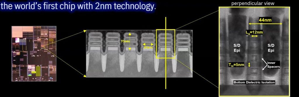
Several novel features are included in the latest 2 nm chip: A novel multi-Vt scheme for both SoC and HPC applications, as well as an industry-first bottom dielectric isolation (see Figure) to allow the 12 nm gate length, a 2nd generation inner spacer dry method for precise gate control, EUV patterning to produce variable nanosheet widths from 15 nm to 70 nm, and an industry-first bottom dielectric isolation (see Figure).
The bottom dielectric isolation, according to Khare, is critical for reducing leakage current. A 300mm silicon bulk wafer was used to build the chip. He explained, “The dielectric provides the leakage current reduction needed to scale gate length to 12 nm.”
Since the 7nm century, EUV technology has been used primarily for middle-of-line and backend interconnects. It’s the first time EUV has been used in the front-end for transistor formation, according to Khare. “Now, EUV lithography can be used for all important features. It effectively adds another knob for our designers, allowing them to have variable sheet widths ranging from 15 to 70 nanometers,” he explained.
According to Khare, the multi-Vt scheme allows threshold voltage control for the “entire spectrum of operation,” from a low-power handheld smartphone app to a high-performance server app in a data center.
The new chip does not employ stacked CMOS nanosheets, but that could be in the future. “Stacked CMOS is among several new device architectures we are exploring,” he said.
For consumers, these chips could potentially lead to cell phones that only need to be charged once every four days by quadrupling the average phone battery life within the same power envelope.
picture courtesy: pcworld.com


Leave a Reply